Here we show you how to simulate and analyze charge transport and excitonics in a fluorescent OLED device. The device setup, consisting of an HTL (red), an EML (host material doped with 2% (mol) emitter) and an ETL is illustrated below.
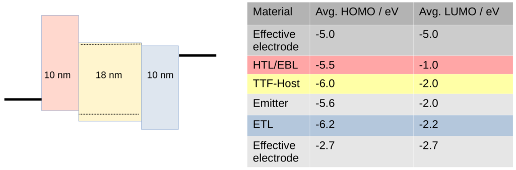
In this system the energy levels are set such that the emitter does only trap holes (not electrons), leading to imbalanced charge transport (electron transport being better than hole transport). In addition, a large singlet-triplet gap is set for TTF-host and emitter. For simplicitly, we did not include doped injection layers explicitly, but used effective electrodes instead. These effective electrodes have enery levels of doped injection layers and require a compensation of the modified built-in voltage. Check out our tutorial on full ab-initio stack simulation to learn how to explicitly include doped injection layers.
Setup
We simulate charge carrier and exciton dynamics of this OLED using our multi-purpose kinetic Monte-Carlo tool LightForge. The following description highlights the most relevant settings. For a general introduction to the LightForge GUI, please refer to the LightForge documentation. Further, you can find this workflow pre-defined in our virtual lab (request a free trial here). For a detailed step-by-step guide, please follow our recorded webinar, which also contains more details on analyzing simulation results.
General and IO:
- In the general-tab, set device_layout to “stack”, set_PBC to “automatic, check “connect_electrodes” and activade all particle types by checking the respective check boxes (electrons, holes and excitons)
- In the IO-tab, disable “use QP output” and “Override Settings”
The most important settings for this use case are in the materials tab. If material properties are not taken from ab-initio calculations (i.e. QP output) you need to supply energy transport levels (IP, EA), energy disorder (sigma) and reorganization energies. Excitonic properties are assigned to materials via presets. Predefined presets are fluorescent, phosphorescent, doping and tadf. These presets can be adapted to modify material parameters.
In this simulation, we define the four materials listed in the table above and set energies respectively. Disorder is set to 90 meV and lambda (reorganization energy) to 200 meV for all materials. For HTL and ETL, set exciton preset to fluorescent. For TTF-Host and emitter, we define a new the high singlet-triplet-gap preset (click “show exciton_presets” and use the plus button to add a new preset) with a singlet decay rate of 2e8 s and a singlet-triplet gap of 1.1 eV, as illustrated below.

With the remaining tabs, proceed as follows:
- device: set morphology width to 20 nm, define all layers and adapt thicknesses according to the illustration above. Make sure to include both host and emitter in the emission layer. Set the electrode workfunctions to -5.0 eV and -2.7 eV (effective electrode, as described above), set coupling model to “parametrized” and increase electrode_wf_decay_length to 0.5.
- Topology: set “max neighbors” to 26, chose “Miller-Abrahams” as transfer integral source and leave FRET as is. Then use the plus button to add a set of pair parameters to all material pairs (HTL-HTL, HTL-TTFHost, HTL-Emitter, TTFHost-TTFHost, TTFHost-Emitter, TTFHost-ETL, Emitter-Emitter, Emitter-ETL, ETL-ETL). Set “maximum_ti” to 0.0001 for only the Dexter transfer integrals of all pairs and leave the rest as is.
- Physics: set rates to “automatic” and uncheck “superexchange”.
- In the Operations tab, set number of simulations to 15 to average over 15 independent runs (disorder configurations) for statistics. Set initial holes and electrons to 0, and chose fields at 0.07, 0.08, 0.09, 0.11 V/nm. Considering the modified in-built voltage of (2.7-5.0) eV, this corresponds to effective fields of 0.012 0.022 0.032 and 0.052 V/nm. Adapt computational parameters as follows: IV_fluctuation: 0.000001; max_iterations: 600000; max_time: 1.0e5.
- In the analysis tab, check “exciton lifecycle”, set autorun_start to 0.1 (tracking will start at 10% of the simulation time) and keep the remaining options disabled.
Now we are ready to go. Allocate up to 61 cores in the resources tab (we have 4 fields with 15 simulations each, plus one master thread) and submit the workflow to your computational resource.
Results
LightForge generates a variety of output files for analysis. In the following, we will present the output most relevant for excitonics analysis in OLED devices. For further information on outputs, please reference the LightForge documentation, watch the webinar, or send us an email. You can get results either by downloading the file “results.zip” from the runtime directory, or locating the submitted workflow in the Jobs&Workflows panel form SimStack and opening files via the SimStack filebrowser (right click on “lightforge2” in the workflow -> Browse directory).
IV and IQE, located in “results/experiments/current_characteristics” are displayed below. We find an internal quantum efficiency of 20% at low fields/current densities, which drops below 10% at high current density.

To investigate microscopic reasons for this roll-off, we analyze the quenching profiles, namely the files “quenching_density_average_*.png”, “photon_creation_density_average_*.png” and “exciton_decay_density_average_*_species_total.png” in the folder “results/experiments/particle_densities/”, where the *=0,1,2,3 correspond to the different fields. These figures are compiled below. Top left: Hole, electron and exciton-quenching densities in red, blue and black respectively; Top right: Exciton creation and emission profile in red and yellow; Bottom left: Excitonic processes over the device cross section with a zoom-in in the bottom right panel at highest applied field.

In this device, excitons are created at the HTL/EML interface. Exciton transport leads to both emission and quenching throughout the EML. As illustrated in the bottom panels, excitons are mainly quenched by interaction with charges and in TTF processes. Comparison to lower fields (not illustrated) reveals that TTF is only significant at high fields.
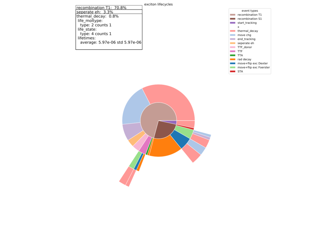
A detailed analyzis of the lifecycle of excitons are available in the interactive files “exciton_lifecycle_*.html”. These pie-charts, illustrated below for a medium field, show states and “conversion” processes an exciton undergoes until gone from the system. Howevering over each section displays details such as occurrence and distribution of molecular species on which these events occur.

These charts are read from the inside out: The innermost fields are the “birth” of an exciton, consisting of ~75% recombination into a triplet and 25% recombination into a triplet. The field “start_tracking” contains excitons (mainly triplets) already exist at the beginning of the tracking analysis. Fields at the edge indicate that excitons are destroyed, e.g. by polaron quenching (“move_charge” in light orange). Going from the triplets in the innermost circle to the second circle, we find that 17.4% of all excitons are destroyed in a TTF-process (labeled “TTF_donor” in cyan) with another 17.4% of excitons (light green) that can continue in their lifecycle (additional layers in this graph), e.g. via STA (7%) and radiative decay (4.7%). Approximately half of the singlets was directly quenched via STA and one third decayed radiatively.
The total radiative decay results from the sum of all green fields. This analysis therefore illustrates, that TTF contributes significantly to the radiative decay and approximately doubles the OLED efficiency at high fields. Comparison to the smallest field illustrated below, however, shows that at low fields, more than two thirds of all triplets are lost due to thermal decay or polaron quenching and TTF very rarely occurs due to the low exciton density. On the other hand, the corresponding low charge carrier density leads to less quenching of singlets and therefore an overall higher IQE than at high fields.
For further ways to analyse your results check out our webinar or refer to the documentation page.