Virtual Design is facilitated by combining multiple software modules in automated bottom up multiscale modeling approach into a predictive, flexible and easy-to-use tool. This tool allows the development of custom-tailored workflows that include single molecule optimization, multistack structural formation, electronic structure calculations and charge transport simulations. The scientific modules are incorporated into the drag-and-drop SimStack workflow environment, minimizing training periods while maximizing scalability.
User manuals and webinars for our software can be found on our documentation page, sample applications in the virtual lab.
To request a trial version, visit the download page.
The standard organic electronic workflow follows four basic steps:
-
- Single molecule parametrization
| The geometries of single molecules (the constituents of e.g. HTL or ETL, host materials, dopants) are optimized on DFT level. Using the Parametrizer module, customized force-fields are automatically calculated on quantum mechanical level for each molecule for optimized structural formation in the next step. |
-
- Generation of atomistic morphologies
| Based on the customized, DFT-based force-fields, thin-films with atomic resolution are generated from the ground up, using Deposit. Parallelized, grid-based force-field evaluation allows the fast deposition of morphologies on the 10 nm scale. By mimicking physical vapor deposition, experimentally observed features, such as inhomogeneities and anisotropies are featured in structures generated by Deposit. | 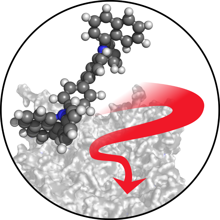 |
-
- Calculation of charge hopping rates
| Atomistic morphologies are fed directly into QuantumPatch for the full quantum mechanical calculation of the electronic structure in molecular layers and at organic interfaces, such as electronic couplings, reorganization and orbital energies. Environmental effects are taken into account, enabling the analysis of pristine layers, doped systems and specific interface effects. | 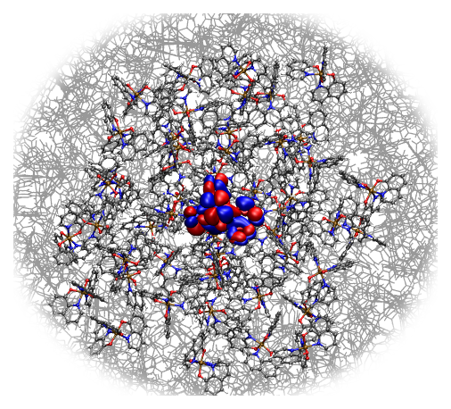 |
-
- Charge transport simulations
| Based on the electronic structure in the molecular layers, charge transport on the device level, from single layers to multi-stack devices, is calculated using the kinetic Monte-Carlo tool LightForge. Taking into account all relevant excitonic and charge transport processes, LightForge allows the detailed analysis of microscopic bottlenecks in device performance. | 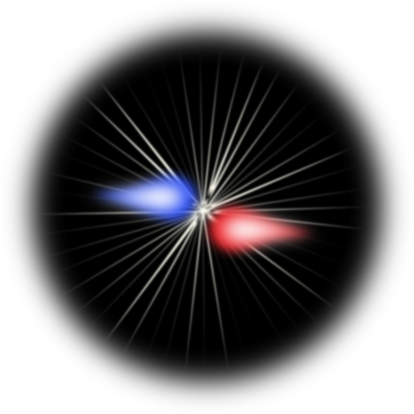 |